MiNaPAD Forum 2019MiNaPAD Forum 2019MiNaPAD Forum 2019MiNaPAD Forum 2019
  • Home
  • IMAPS
    • BULLETIN ADHESION IMAPS FRANCE
    • Chapters
    • Jobs
    • Advancing Microelectronics
  • Events
    • Events Archiv
  • News
    • IMAPS-France Infos
    • News from IMAPS EUROPE
  • Members Area
    • Archives
    • Photo Gallery
  • IMAPS EU
✕
  • Home
  • Events
  • MiNaPAD Forum 2019

MiNaPAD Forum 2019

Micro/Nano-Electronics Packaging & Assembly, Design and Manufacturing Forum

MiNaPAD, the « Micro/Nano-Electronics Packaging & Assembly, Design and Manufacturing Forum » will be held in Grenoble, France, at the WTC congress center on May 22-23, 2019.

MiNaPAD is a 2 days conference with an exhibition. The objective of this event is to reinforce the design community (which constitutes the largest share of the semiconductor community in Europe) and the assembly and packaging community:

  • parallel technical sessions
  • an exhibition
  • additional  technical events (May 21, 2019)

Download the program here.

Click here to register for MINAPAD 2019.

  • Venue
  • Exhibition
  • Program

Venue

ACCOMMODATIONS

ACCESS MAP


By train

  • Train station at 100m of Congress center
  • Several daily connections with Europe’s big cities:
  • Grenoble-Paris: 10 direct TGV high speed trains, in 3 hours
  • Grenoble-Lille-Bruxelles: 1 TGV high speed train per week, in 5.5 hours
  • Grenoble-Paris-Cologne: 4 TGV high speed trains per day, in 8 hours
  • Grenoble-Turin-Milan: 3 round trips per day;

By road

A crossroads, Grenoble is particularly easy to access? Arrival by motorways A48 (Lyon, Valence), A41 (Chambery, Annecy), and A51 (Marseille)

A few distances

  • Grenoble-Paris: 574 km
  • Grenoble-Nice: 343 km
  • Grenoble-Strasbourg: 535 km
  • Grenoble-Geneva: 147 km


Categories Number Capacity
Hotel**** 2 55
Hotel*** 23 1420
Hotel** 50 1868
Hotel* 6 586
Total 81 3929


Plane


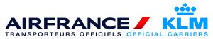
Attractive discounts, up to -15%, on a wide range of public fares on all AIR FRANCE, KLM and their code-shared flights worldwide.

Event: MINAPAD2019

ID Code: 34936AF

Travel Valid Period: 15/05/2019 to 30/05/2019

Event location: Grenoble


Please visit the event website or access directly through http://globalmeetings.airfranceklm.com/Search/promoDefault.aspx?vendor=AFR&promocode=34936AF


Grenoble Airport Isère 40 minutes

http://www.grenoble-airport.com


Railway station-Airport every three hours from 5.15 am to 6.05 pm Time 45mn

Airport-Railway station every three hours from 10.10am to 10.30 pm

Lyon St Exupery Aiport  distance 50 minutes

http://www.lyon.aeroport.fr


Shuttles:

Airport-Grenoble every hour 7.30 am to 7.00pm

Time 1 hour

Grenoble-Airport every hour 5.00 am to 7.00

Time 1 hour


Geneve Airport Cointrin distance 1.30 pm

http://www;gva.ch

Shuttles

Airport –Grenoble every 3 hours 8.30 am to 7.30 pm time 2 hours

Grenoble-Airport every 3 hours 6.00 am to 4.00 pm time 2 hours


Local Transport

Tramway

Line A Stop Railway station

Line B Stop Palais de Justice


Parking

Europole Railway Station 600 places, rue du Doyen Louis Weil

Le Doyen 400 places, rue du Doyen Louis Weil

Exhibition

EXHIBITION INFORMATION

EXHIBITION REGISTRATION

METRONELEC
HYBRID S.A.
POLY DISPENSING SYSTEMS
BT ELECTRONICS
FT POLYMER
PREDICTIVE IMAGE
NGK/NTK
MSE
TAIPRO ENGINEERING
KYOCERA
AEMTEC
EGIDE
ELEMCA
MICROSS COMPONENTS
PROTAVIC
HCM SYSTREL GROUPE SERMA
ASE
 ACCELONIX
 SURON
 ISP SYSTEM
 JCET/STATS CHIP PAC
 MICROTEST
 JFP MICROTECHNIC
 ELECTRON MEC
 VALTRONIC
 PLASMA-THERM
 DISCO HI-TEC Europe GmbH
 TELEDYNE E2V
 COOKSON
 ESIEE

Program

MiNapad 2019 


Tuesday May 21st

15h30 to 17h30 Lecture Subramanian S. lyer

(Samueli School of Engineering, University of California, Los Angeles USA) Makalu Room

Packaging- When all else fails! Or Why I became a packaging Engineer

Co-Organized with  


Wednesday May 22nd

8h45                     Welcome to MiNaPAD

9h00                     Opening by Alexandre Val (Auditorium)

9h30                    Keynote 1: Subramanian S. lyer

“A Moore’s law for packaging” (Auditorium)


10h15                  Exhibition Opening (Exhibition Hall)

Session A : MEMS & LED Session B : Process Optimization
10h45 CMOS Image Sensor Packaging Technology (T.E. Kang, UTAC Group) Copper Wire Robustness for High Volume Production

(F. Quercia, ST Microelectronics)

11h10 Curved Full-Frame CMOS Sensor: Impact on Electro-Optical Performances

(B. Chambion, CEA-LETI)

Packaging for the Automotive Industry

(L. Chemisky, YOLE Développement)

11h35 A New Method for a Failure Characterization of a Flip-Chip Assembly of pixelated LED Light Source Package

(S. Beddar, Versailles Saint-Quentin University)

Adhesion strength of Epoxy Molding Compound to metals in a semiconductor package (F. Viviani, St Microelectronics)
12h00–13h15 Lunch (Exhibition Hall– Exhibition)
13h15 Keynote 2: Jacques Fournier (CEA-LETI): Secure Packaging for Addressing Hardware Security Challenges (Auditorium)
Session C : Interposer 2.5D/TSV/3D Session L: Specific topics
14h30 New Copper and Cobalt wet metallization enabling multiple Integrations for FEOL and BEOL (M. Baus, AVENI) Electronics in Europe

(Olivier Coulon, DECISION)


14h55 Layout Design of I/O Libraries for Wirebond & Flip-Chip Package options

(K. Chanumolu, ARM)

Backside Protection against physical attacks for secure chips or SiP

(S. Borel, CEA LETI)

15h20 Metrology for High Density Wafer Level Fan-Out & TSV based stacking

(D. Alliata, UNITYSC)


15h45 Advanced Packaging Material Developments for 3D Stacking and System-In –Package

(R. De Witt, Henkel Electronics Materials

16h10-16h35 Exhibition/coffee break sponsored by


Session D : Dicing/Picking 1 Session E : PCB1-Embedded


16h35 Plasma Dicing: A Device-Enabling Technology for advanced Packaging and 3D Integration

(P. Bezard, PLASMA-THERM)

EHDICOS “Embedded Technologies” with standards Components

(F. Lechleiter, CIMULEC)

17h00 A more than Moore Enabling Wafer Dicing Technology

(J. van Borkulo, ASMPT)

EDDEMA: Embedded Die Design Environment and Methodology for Automotive Applications

(N. Marier, VALEO)

17h25 Development of Back Gridding/Mask 2 in 1 Tape for Plasma Dicing Process

(T. Uchimaya, FURUKAWA ELECTRIC)

Advanced PCB Technology for Integrated Flexible Electronics

(J. Verhegge, ACB)


17h50-18h30     Exhibition

19h30                  Social Event – Restaurant “Les Jardins de Sainte Cécile”

Cette photo par Auteur inconnu est soumis à la licence CC BY-SA-NC

18h30 – 19h30 Extra: Visit of Rembrandt exposition located close to Social event and sponsored by CEA LETI – Please booked it due to limited to 25 persons (English language guide).

Thursday May 23rd


8h30                     Keynote 3: Jean-Marc Yannou (ASE): Car Electrification: a revolution also for the

semiconductor packaging marketing (Auditorium)

Session F : Characterization/Reliability Session G : Advanced Process
9h30 Mechanical Behavior of SAC305 Lead free Alloy (J. Vieilledent, THALES Global Services) Innovative Implementation of additive Manufacturing for Advanced Microelectronics Packaging

(A. Roshangias, CTR)

9h55 Thermomechanical Behavior Characterization new Development for high Resolution multi-scale Analyses

(D. Ecoiffier, INSIDIX)

Increased Integration Density of optoelectronic Modules by Through-Silicon Laser Soldering adapted for Wafer Level Packaging (S, REINKEN, FICONTEC)
10h20 A comprehensive Methodology for Design for Package Miniaturization

(R. Duca, ST Microelectronics)


Moisture uptake of PECVD dielectrics at ambient and accelerated Test Conditions

V. Cartaillier, (Laboratory IMS & ST Microelectronics)


10h45-11h10     Exhibition/coffee break sponsored by 

Session H : SiP Session I : Joining/Advanced Process
11h10 Miniaturized Medical Devices

(P. von Meiss, VALTRONIC)

Statistical Study of SAC Solder joints in QFN and BGA assemblies

(H. Fremont, Laboratory IMS)

11h35 Evolution of RF SiP and challenges ahead

(C. Zinck, ASE)

Key Advances In Void Reduction and Warpage Mitigation in the Reflow Process (J. Balackyi, HELLER Industries)

12h00– 13h00   Lunch & Exhibition (Exhibition hall)

13h00                  Keynote 4: Dr. Hannes Voraberger (AT&S): Microelectronics and Integration Technologies:

Enabler for Smart Mobility (Auditorium)

  Session J : PCB2-Power Session K : Dicing/Picking 2
13h35 High Power PCB for air plane applications (G. Belijar, IRT) Sawing Capability Study for Front-Side Chipping Reduction (M. Tumiati, ST Microelectronics)
14h00 Double Side Interconnection for vertical power components based on Macro and Nano structured Copper Interfaces and printed Circuit Board Technologies

(B. Djuric, MITSUBISHI Electric)

Packaging of a MOEMS LIDAR Sub Assembly for distance Metering on a 3D housing

(J. Abdilla, BESI AT)


14h25 Thermal Management in the PCB

(S. Houivet, ELVIA)


Laser-lift-off (LLO) and CONDOx for Wafer ultra-thinning process for 3D stacked Devices, TSV, eWLB and WLCSP and DICING WITHOUT Adhesives for MEMS and optical devices (G. Klug, DISCO)

15h00-15h20     Exhibition / Coffee Break


15h20                  Keynote 5: YOLE/SYSTEM PLUS To be completed (Auditorium)

16h15                  Best Paper Awards sponsored by 


16h30                  End of MiNaPAD2019

Sponsors

ST_Logo_Standard_9Jan
ASElogo
CEA - Commissariat à l'énergie atomique et aux énergies alternatives
Share

Event-Details

Date

22 May 2019 - 23 May 2019

Location

Grenoble, France, at the WTC congress center


Program
Become a Member!
IMAPS Europe. All Rights Reserved | Privacy Policy | Imprint